Taalas Tokens Per Second Per User Comparison
TL;DR: The Taalas Revolution in 60 Seconds
-
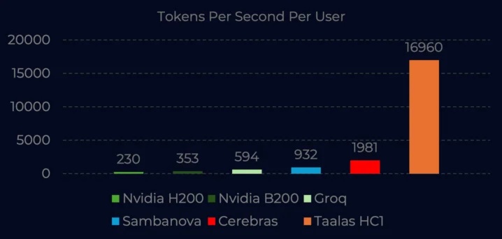
The Breakthrough: Taalas has unveiled the HC1 chip, achieving a massive 17,000 tokens/second on Llama 3.1 8B. It is roughly 10x faster and 20x cheaper than traditional GPU inference.
-
The “Hardwired” Secret: Unlike GPUs that load software, Taalas etches the AI model directly into the silicon transistors. By physically embedding the weights, they eliminate the need for High-Bandwidth Memory (HBM).
-
Solving the Memory Wall: By removing the “data movement” between external memory and the processor, Taalas bypasses the industry’s biggest bottleneck—the Memory Wall—and operates entirely on standard air cooling.
-
The Trade-off: The chip is model-specific. While it offers “insane” efficiency for stable, high-volume production (like 24/7 chatbots), it lacks the programmability and flexibility of a GPU.
-
Market Impact: The rise of these specialized “Inference Factories” actually increases the long-term value of your GPUs. Because GPUs are versatile and can be repurposed for any new model, they remain the “Gold Standard” for resale and training.
- Demo LLM: chat jimmy
==========================
The year 2026 has brought the AI industry to a critical crossroads. For the last three years, the narrative of “more is better”—more parameters, more data, and more GPUs—has collided head-on with the physical and economic reality of the Memory Wall. As of early this year, the global supply of High-Bandwidth Memory (HBM) remains the single tightest bottleneck in the AI supply chain, driving lead times for general-purpose accelerators to unprecedented lengths and inflating the Total Cost of Ownership (TCO) for enterprise inference.
Against this backdrop, a Toronto-based startup called Taalas has emerged from stealth with a proposition that sounds like a fundamental rewrite of semiconductor physics: an AI chip that doesn’t just run software, but is the software. By announcing its HC1 accelerator, which claims a staggering 17,000 tokens per second (TPS) on Llama 3.1 8B, Taalas is betting that the only way to solve the memory crisis is to eliminate traditional memory altogether.
For IT directors and infrastructure strategists, this is the most significant architectural divergence in a decade. It forces a hard question: Is the future of the data center still programmable, or are we entering an era of “Hardcore AI” appliances?
What is the Taalas HC1 Chip? The “Model-as-Silicon” Architecture
The Taalas HC1 is an Application-Specific Integrated Circuit (ASIC) that represents a radical departure from the Von Neumann architecture used by NVIDIA, AMD, and Intel. In a traditional system, a processor (CPU/GPU) fetches instructions and data from memory, processes them, and sends them back. The HC1 discards this “fetch-and-execute” cycle.
Instead, Taalas utilizes a “direct-to-silicon” foundry process. The architecture of a specific model—in this first instance, Meta’s Llama 3.1 8B—is physically etched into the transistors of the chip.
Key Technical Specifications of the HC1:
-
Performance Benchmarks: Internal and early third-party testing shows the HC1 hitting 14,357 to 16,960 tokens per second, nearly two orders of magnitude faster than a single NVIDIA H200 in a comparable single-stream scenario.
-
Transistor Density: Manufactured on TSMC’s 6nm (N6) process, the chip packs 53 billion transistors into an 815mm² die—maximizing the reticle limit of the 6nm node to prioritize on-chip storage.
-
Power and Cooling: Each card draws approximately 200W to 250W, allowing for a server with ten HC1 cards to run at 2.5 kW. Crucially, it requires only standard air cooling, removing the infrastructure hurdle of liquid-cooled racks.
-
Zero HBM Dependency: The chip uses zero external High-Bandwidth Memory (HBM). By embedding model weights in a custom Mask ROM recall fabric, the data never has to leave the silicon die.
Unlike traditional hardware that “loads” a model into memory, Taalas uses what they call a “direct-to-silicon” foundry process. The model’s weights and architecture are literally printed onto the upper metal layers of the chip. This results in a processor where “the model is the computer.”
Why Is This Innovation Gaining Such Intense Attention?
In 2026, the AI market has matured. We are no longer just asking “Can we build it?” but “Can we afford to run it?” This shift from training to inference is the primary reason Taalas has captured the industry’s imagination.
1. The Inference-to-Training Pivot
By mid-2026, inference workloads are expected to account for nearly two-thirds of all AI compute. While GPUs are essential for the flexible, iterative work of training, they are increasingly seen as an expensive overkill for serving a stable, production-ready model like Llama 3.1. Taalas targets the “Inference Factory”—data centers designed to serve billions of tokens daily at the lowest possible cost.
2. The Total Cost of Ownership (TCO) Collapse
The economic claims are perhaps more startling than the performance figures. Taalas asserts that their approach drops the cost of inference to roughly 0.75 cents per million tokens, compared to the 20–49 cents typical of high-end GPU clusters. For an enterprise serving millions of customers, this represents a 20x to 50x reduction in operational expenditure.
3. Freedom from the HBM Shortage
Traditional AI accelerators are currently held hostage by the global supply of High-Bandwidth Memory (HBM). HBM is expensive, difficult to manufacture, and accounts for a significant portion of a GPU’s bill of materials. By hardwiring weights into the silicon, Taalas completely eliminates the need for HBM. This not only lowers the price but simplifies the supply chain, allowing for faster scaling in an environment where HBM remains a critical bottleneck.
Why Is This Innovation Gaining Such Intense Attention?
By mid-2026, inference workloads are expected to account for nearly two-thirds of all AI compute. While GPUs are essential for the flexible, iterative work of training, they are increasingly seen as an expensive overkill for serving a stable, production-ready model like Llama 3.1. Taalas targets the “Inference Factory”—data centers designed to serve billions of tokens daily at the lowest possible cost.
In the world of IT procurement, “fast” is good, but “efficient and available” is better. The Taalas announcement has gained traction not just because of the 17,000 TPS figure, but because it addresses the three systemic crises facing the 2026 data center: cost, power, and the HBM shortage.
1. The Death of the “Inference Tax”
Currently, companies pay an “inference tax” to run their models. Serving a million tokens on a GPU-based cloud provider costs between 20 and 50 cents. Taalas claims its HC1 can deliver the same volume for roughly 0.75 cents. For enterprises deploying AI agents at scale, this is not an incremental gain; it is a 50x reduction in operational cost that fundamentally changes the economics of AI-driven business models.
2. Bypassing the Global HBM Shortage
The AI boom has created a massive shortage of HBM3 and HBM3e memory, which is currently the most expensive component of an AI server. By hardwiring weights into the transistors, Taalas is essentially “printing” its own memory. This allows the company to scale production without competing for the same constrained memory wafers as NVIDIA and AMD, potentially offering much shorter lead times for high-volume deployments.
3. The Pedigree of “Hardcore AI”
This isn’t a speculative venture from a software-only startup. Taalas was founded by Ljubisa Bajic, the architect behind Tenstorrent and a veteran of NVIDIA and AMD. His team of 25 engineers has brought this chip to market with just $30 million in R&D spend—a fraction of what traditional semiconductor firms spend—demonstrating a highly optimized foundry workflow that can turn a new model into hardened silicon in just 60 days.
The Core Technical Innovation: Solving the Memory Wall
To understand why Taalas is so fast, one must understand the “Memory Wall”—the fundamental bottleneck of modern computing. In a standard von Neumann architecture (which includes GPUs), the units that calculate (compute) are separate from the units that store (memory).
The Data Movement Tax
In traditional inference, every time a model generates a token, it must fetch billions of parameters from HBM, move them across a bus to the compute cores, perform the math, and then move them back. This data movement accounts for 80–90% of a chip’s energy consumption and the vast majority of its latency.
The Mask ROM Recall Fabric
Taalas solves this by merging storage and computation into a single physical structure. They use a proprietary “Mask ROM recall fabric” to store the model weights.
-
Weights as Transistors: Instead of bits stored in a separate RAM chip, the weights are represented by the physical configuration of transistors and metal interconnects on the HC1.
-
Compute-on-Storage: Computation happens at the location of the data. There is no “fetching.” The signal simply flows through the hardwired weights, producing an output in a single pass.
-
Digital Accuracy: Despite sounding like an analog approach, Taalas remains fully digital, utilizing a “one-transistor-per-weight” density that allows 8 billion parameters (in quantized formats) to fit on a single die.
Technical Insight: The HC1 isn’t completely unchangeable. It includes a programmable SRAM recall fabric that supports Low-Rank Adaptation (LoRA) and fine-tuning. This allows users to bake in a base model (like Llama 3.1) while still being able to “patch” it with specialized company knowledge or safety filters.
The Strategic Trade-off: Specialization vs. Versatility
We must balance our excitement with a dose of candor. If Taalas is so efficient, why hasn’t everyone moved to “Hardcore AI”? The answer lies in the trade-off between efficiency and agility.
The Case for Specialization (The Empathy)
For organizations that have “found their model,” the GPU is a wasteful tool. If you are a global bank using a specific 8B model for 100% of your automated customer interactions, you don’t need a chip that can also render Cyberpunk 2077 or train a weather model. You need a dedicated appliance. In this context, the HC1 is the “network switch” of AI—a piece of infrastructure you set, forget, and let run with maximum efficiency.
The Case for Versatility (The Candor)
The “blind spot” for many looking at ASICs is model volatility. AI architectures are evolving at a breakneck pace. If a new model architecture—such as a State Space Model (SSM) or a revolutionary Mixture-of-Experts (MoE)—suddenly makes Llama 3.1 obsolete, a “Hardwired Llama” chip becomes a very expensive paperweight.
-
Rigid Lifecycle: While Taalas claims they can move from a new model to a finished chip in roughly 60 days by changing only two metal layers, that is still an eternity compared to a 60-second software update on an NVIDIA GPU.
-
Training Dependency: You cannot “hardwire” a model until it is finished. This means the world will always need GPUs to discover the “next big thing” before companies like Taalas can cast it into silicon.
Impact on ITAD and the Secondary Market
As an IT asset disposition (ITAD) leader, we look at the Taalas news through the lens of residual value and hardware lifecycle management.
-
GPU Liquidity: The general-purpose GPU (like the H100 or Blackwell) remains the “Blue Chip” asset of the data center. Its versatility ensures that even after three years of use, it can be resold to any industry for training, 3D rendering, or different AI models.
-
ASIC Depreciation: Specialized chips like the Taalas HC1 will likely depreciate more like networking hardware or proprietary storage arrays. Their value on the secondary market will be tethered to the longevity of the model they support.
-
The Segmentation of Assets: We are entering a phase where data centers will have two distinct tiers of hardware: Universal Compute (GPUs for training/R&D) and Fixed Inference (ASICs for high-volume production). Managing the end-of-life for these two categories will require entirely different disposition strategies.
Strategic Insight for IT Managers: The rise of specialized silicon doesn’t make your GPUs less capable—it makes them more valuable to the millions of organizations that still require programmable flexibility for training and R&D.
As the industry begins to segment into these specialized niches, now is the ideal time to audit your infrastructure. If you are preparing to transition your “inference factory” to specialized ASICs, we can help you recoup maximum value from your versatile general-purpose fleet. We offer industry-leading bulk gpu buyback programs designed to turn your surplus hardware into liquid capital, allowing you to reinvest in the next generation of AI compute without the burden of depreciating legacy tech.
Conclusion: A New Paradigm for 2026
The Taalas HC1 isn’t just a faster chip; it is a solution to the most expensive bottleneck in modern computing. By solving the Memory Wall through physical hardwiring, it provides a glimpse into a future where AI tokens are as cheap and ubiquitous as electricity.
While the GPU will remain the undisputed king of the research lab and the training cluster, the “Inference Factory” of the future will likely run on specialized silicon. As these new assets begin to enter the enterprise lifecycle, the key to a successful infrastructure strategy will be balancing the high-performance “rigidity” of ASICs with the safe “liquidity” of versatile GPUs.