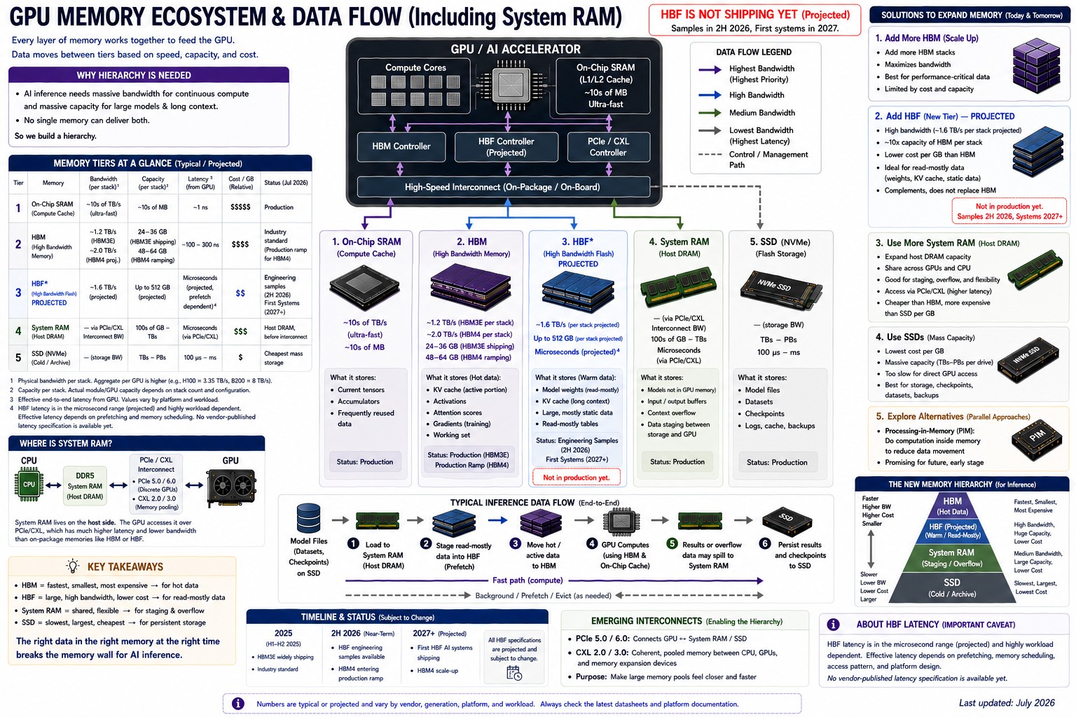
How data actually moves through an AI server, why HBM became the industry’s tightest bottleneck, and where projected technologies like High Bandwidth Flash and CXL fit into the picture.
The diagram shows the typical staged path. On systems configured with GPUDirect Storage, NVMe drives can DMA data directly into HBM, bypassing the System RAM hop.
The common mental model of AI hardware goes something like this: a GPU loads the model into its memory, then starts computing. Simple. It is also wrong in almost every detail that matters.
A modern AI server contains an entire hierarchy of memory technologies, each engineered for a different balance of speed, capacity, and cost. Some of these memories respond in billionths of a second and cost so much per gigabyte that they are measured out in megabytes. Others store petabytes cheaply but respond thousands of times more slowly. None of them can do the whole job alone.
Understanding how these layers cooperate explains a lot of things that otherwise look mysterious: why data-center GPUs carry six-figure price tags, why high-bandwidth memory has become the single tightest constraint in AI infrastructure, and why NVIDIA, AMD, Samsung, Micron, SK hynix, and SanDisk are all pouring billions into memory technologies most people have never heard of.
Here is the hierarchy at a glance, fastest and smallest at the top. Each tier is unpacked below.
| Memory tier | Bandwidth | Typical capacity | Primary AI function |
|---|---|---|---|
| On-chip SRAM | Fastest in the system; nanosecond access | Kilobytes to megabytes | Tiles of data being computed right now |
| HBM3E / HBM4 | 1.2+ TB/s per stack; up to 8 TB/s per GPU shipping today | 36 GB per stack; up to 288 GB per GPU | Active model weights, activations, KV cache |
| HBF (projected) | Up to 1.6 TB/s read per stack (target) | Up to 512 GB per stack (target) | Read-mostly weights and long-context data |
| System RAM (DDR5 / LPDDR5X) | Tens of GB/s per channel; up to 1.2 TB/s in tightly coupled designs | Hundreds of GB to terabytes | Staging, overflow, KV-cache offload |
| CXL-pooled DRAM | Link-limited; slower than local DRAM | Terabytes, shared across hosts | Warm capacity: spilled caches, retrieval indexes |
| NVMe SSD | Roughly 14 GB/s per PCIe 5.0 drive | Terabytes to petabytes | Models at rest, checkpoints, datasets |
Why one memory can’t do it all
Picture a line cook during a dinner rush. The cook’s hands are the GPU cores. Whatever is being chopped right now sits on the cutting board. Ingredients for the next few dishes wait on the counter. The walk-in refrigerator holds everything needed for tonight’s service, and the dry-storage pantry in the back holds bulk supplies for the week.
No sane kitchen keeps the entire pantry on the cutting board. There isn’t room, and most of it isn’t needed this second. Instead, ingredients flow forward as they’re needed: pantry to walk-in, walk-in to counter, counter to board. Every step farther from the cook’s hands means more walking and more waiting.
Computers are organized the same way, for the same reason. Fast memory is expensive and physically small; large memory is cheap and slow. So instead of one giant pool, an AI server arranges its data in layers, and the whole engineering game is keeping the GPU’s “cutting board” stocked so those absurdly expensive cores never sit idle.
The layers, from fastest to largest
On-chip SRAM: registers and caches
The fastest memory in the system lives on the GPU die itself: registers, L1 cache and shared memory inside each streaming multiprocessor, and a larger L2 cache shared across the chip. This is SRAM, and it responds in nanoseconds. It is also tiny. Where HBM is measured in gigabytes and SSDs in terabytes, on-chip SRAM is measured in kilobytes and megabytes, because each SRAM cell needs six transistors and eats die area that could otherwise hold compute units.
That scarcity shapes how AI software is written. Techniques like FlashAttention exist precisely to restructure attention math so intermediate results stay in on-chip SRAM instead of making round trips to HBM. When a kernel is tuned well, data gets reused many times per visit to the chip. When it’s tuned badly, the GPU spends its life waiting.
HBM: the working memory beside the GPU
High Bandwidth Memory is what people usually mean when they talk about a data-center GPU’s memory capacity. It is DRAM, but packaged in a way ordinary DRAM never is: multiple dies stacked vertically, connected through the stack by thousands of vertical channels called through-silicon vias (TSVs), and mounted millimeters from the GPU die on a slice of silicon called an interposer.
That short, extremely wide connection is the entire point. A conventional DDR5 module talks to a CPU over a 64-bit channel; an HBM3E stack talks to a GPU over a 1,024-bit interface. Current 12-high HBM3E stacks hold 36 GB and deliver more than 1.2 TB/s of bandwidth per stack. Put eight of those around a GPU and the numbers get large fast: NVIDIA’s Blackwell Ultra (B300) carries 288 GB of HBM3E at 8 TB/s of aggregate bandwidth.
The next step is already defined. JEDEC published the HBM4 standard (JESD270-4) in April 2025, doubling the interface to 2,048 bits and supporting up to 2 TB/s per stack. SK hynix has already completed HBM4 development and readied mass production, with parts that run faster than the baseline spec. NVIDIA’s Rubin GPU, sampling in late 2026, pairs 288 GB of HBM4 with up to 22 TB/s of aggregate memory bandwidth.
HBM’s advantages are bandwidth and energy per bit moved. Its disadvantages are just as clear: it is expensive to make, hard to package, capped in capacity per GPU, and chronically short in supply. More on all of that below.
Host system RAM: the staging area everyone forgets
Here is something that surprises people: an “AI server” still leans heavily on ordinary DDR5, the same basic technology found in office desktops. The CPU owns this memory, and there is a lot of it, often terabytes per socket, at a fraction of HBM’s cost per gigabyte. The GPU reaches it across PCIe or, increasingly, across coherent links designed for the job.
The catch is distance. A PCIe 5.0 x16 slot moves roughly 64 GB/s in each direction, which sounds like a lot until it’s compared with the 8,000 GB/s the GPU enjoys locally. Latency is worse too. So system RAM serves as the staging area: datasets get loaded and preprocessed there, model weights pass through it on their way to the GPU, and workloads that overflow HBM spill into it as a slower safety valve.
Tightly coupled designs are shrinking that penalty. NVIDIA’s Vera CPU pairs up to 1.5 TB of LPDDR5X with a 1.8 TB/s coherent NVLink-C2C link to the Rubin GPU, letting software treat CPU memory and HBM as one address space and offload inference state into the larger, cheaper pool. That design choice alone says a great deal about where the industry thinks the pressure is.
NVMe SSDs: the pantry
At the bottom of the hierarchy sit NVMe SSDs, which are enormous and cheap by comparison and, in this context, slow. A fast PCIe 5.0 drive tops out around 14 GB/s sequential reads; against HBM that’s roughly a five-hundredfold gap. SSDs store model weights at rest, training checkpoints, and the raw corpora used to build datasets.
One point worth being precise about: a GPU never executes directly from an SSD. Data must land in HBM before a tensor core touches it. The route it takes, though, has gotten shorter. In the classic path, data bounces through a buffer in system RAM on its way to the GPU. NVIDIA’s GPUDirect Storage removes that detour, letting NVMe drives DMA data straight into GPU memory over PCIe and skipping the CPU bounce buffer entirely, which cuts latency and frees the CPU for other work. The hierarchy still holds; the ladder just has an express rung for storage-to-GPU transfers.
How the data actually moves
Follow one inference request through the hierarchy shown in the infographic: from NVMe SSD through system RAM into HBM, then through on-chip SRAM to the tensor cores, with results flowing back down.
Model weights start on SSD. At load time they’re staged through system RAM and copied into HBM, or, on systems configured for GPUDirect Storage, transferred by DMA straight from NVMe into GPU memory without the system-RAM stop. Either way they end up resident in HBM while the model serves traffic. During each computation, small tiles of weights and activations move from HBM into on-chip SRAM, get consumed by the tensor cores, and produce outputs that flow back down. Well-built software pipelines these transfers so copying and computing overlap, prefetching the next tile while the current one is being chewed through.
That resident middle layer, HBM, is where the projected High Bandwidth Flash technology aims to insert itself: a new rung between system RAM and HBM for data that is read constantly but written rarely. More on that shortly.
Why HBM became the AI bottleneck
Three forces converged on HBM at once.
First, models outgrew it. Frontier models from the GPT and Llama families, and mixture-of-experts designs like DeepSeek’s, run to hundreds of billions or trillions of parameters. Even quantized, a big model consumes hundreds of gigabytes before serving a single request, which is why it gets sharded across eight or more GPUs whose combined HBM can hold it.
Second, inference created a new memory hog: the KV cache. During text generation, a model stores intermediate attention state for every token in the context window, and this cache grows linearly with context length. The numbers are sobering. A single Llama 3 70B request with a 128K-token context needs about 42 GB of GPU memory for KV cache alone. A handful of long-context users can exhaust a flagship GPU’s memory without the model weights growing by a byte.
Third, token generation is bandwidth-bound. Producing each output token means streaming a large fraction of the model’s weights past the compute units. The arithmetic itself is often the easy part; feeding it is the hard part. That’s why every GPU generation leads its spec sheet with memory bandwidth, and why the industry keeps paying whatever HBM costs.
And it costs plenty. HBM production is effectively sold out, and Samsung and SK hynix have warned that AI-driven memory shortages could persist into 2027 and beyond, with customers reserving supply years in advance.
Why can’t they simply install more HBM?
If HBM is the constraint, the obvious question is why a GPU can’t just carry more of it. The answer is a stack of physical and economic limits, each unforgiving on its own.
Packaging real estate comes first. HBM must sit on the silicon interposer, millimeters from the GPU die, and interposers can only be manufactured so large. Every stack competes for shoreline around the GPU.
Then there’s the vertical dimension. Each stack is 8, 12, or 16 DRAM dies bonded together and connected by TSVs. Every added layer makes the stack harder to build, harder to test, and more likely to fail; one bad die can compromise the whole stack, so yield losses compound with height.
Heat makes it worse. HBM stacks sit beside kilowatt-class GPU packages, and DRAM dislikes heat. Dies buried mid-stack are difficult to cool, and taller stacks deepen the problem. Power is its own budget item too, since every gigabyte and every gigabit per second draws from a rack power envelope that is already the binding constraint in many data centers.
The result is that HBM capacity per GPU rises in disciplined generational steps, not leaps: 80 GB on the H100, 141 GB on the H200, 192 GB on the B200, 288 GB on Blackwell Ultra and Rubin. Each step costs enormous engineering effort. Nobody gets to shortcut it with a bigger shopping cart.
Those steps carry a financial rhythm too. Every generation that ships pushes a wave of previous-generation hardware out of production racks, and organizations funding a B200- or B300-class upgrade often offset part of the cost by selling the H100-era GPUs, memory, and servers being displaced, hardware that still has plenty of working life in a supply-constrained market.
Future technology #1: High Bandwidth Flash (HBF)
This is the newest idea on the board, and worth stating plainly up front: HBF is a projected technology. It is not shipping in any product today, and every figure attached to it is a target, not a measurement.
The concept is to take NAND flash, the technology inside SSDs, and package it like HBM: stacked dies, TSVs, mounted on the interposer next to the GPU. SanDisk and SK hynix signed an agreement in August 2025 to develop the specification jointly, and in February 2026 they moved standardization into the Open Compute Project, an unusual show of cooperation between two competitors.
The pitch is capacity. First-generation targets call for up to 1.6 TB/s of read bandwidth and up to 512 GB per 16-die stack, roughly 8 to 16 times the capacity of an HBM stack at a comparable cost. For read-mostly inference data, model weights that are written once and read billions of times, or long-context KV state, that trade could be compelling. The cost implications for inference workloads are explored further in this look at HBF economics.
The limitations are inherent to flash. Writes are far slower than reads, endurance is finite, and latency is worse than DRAM. Nobody proposes HBF as an HBM replacement; the plan is a new tier beneath it, holding the read-heavy bulk while a smaller amount of true HBM handles hot, frequently written data. The sampling window is now open: SanDisk targets its first HBF samples in the second half of 2026, with a pilot production line reportedly coming online around year-end and the first AI inference devices using HBF expected to sample in early 2027. Until working silicon is in customers’ hands, every figure above remains a target.
Future technology #2: CXL memory expansion
Compute Express Link attacks the capacity problem from a different direction: instead of putting more memory on the GPU package, it puts more memory in the server, or the rack, and lets processors share it coherently. A CXL expansion module or chassis full of DRAM can add terabytes that multiple hosts and accelerators treat as one pool, at DDR5 prices rather than HBM prices.
The standard is moving quickly. The CXL Consortium released CXL 4.0 in November 2025, doubling signaling speed to 128 GT/s, and silicon vendors are building the plumbing: Marvell’s latest CXL switch is aimed squarely at rack-level memory pooling for AI clusters.
The trade-off is latency. Reaching across a CXL fabric costs meaningfully more time than touching local DRAM, so pooled memory suits warm data, spilled KV caches, retrieval indexes, vector databases, rather than anything latency-critical. Software support is still maturing as well. CXL doesn’t replace HBM or local DDR5; it gives overflow somewhere cheaper to live.
Future technology #3: Processing-in-Memory (PIM)
PIM inverts the whole premise of the hierarchy. Instead of moving data to the compute, it moves a little compute into the memory, embedding small arithmetic units inside DRAM banks so simple operations happen where the data already sits, with only results traveling back.
Samsung’s HBM-PIM puts AI engines inside each memory bank and claims roughly double system performance with more than a 70% cut in energy consumption for suitable workloads. SK hynix has demonstrated GDDR6-AiM, which it says speeds up certain computations as much as sixteenfold. The physics favor the idea, since moving data often burns more energy than computing on it. The obstacle is software: decades of code assume memory just stores things, and PIM remains a technology of demos and pilot deployments rather than mainstream AI servers.
Future technology #4: faster HBM, on schedule
The least speculative future is more of the same, executed harder. HBM4 is ramping through 2026 to feed the Rubin generation, and the follow-on is already visible: SK hynix has shipped samples of 12-layer HBM4E to customers. Beyond that, roadmaps point to higher pin speeds and denser stacks, and packaging advances like hybrid bonding promise taller stacks with better thermals. The bandwidth-and-density treadmill has run for a decade and shows no sign of stopping. It just never runs fast enough to make the rest of this article unnecessary.
Putting the whole hierarchy together
Fold the projected pieces in, and the AI server of the next few years matches the table at the top of this article, with one new rung: HBF slotting in between host memory and HBM as a read-mostly capacity tier.
The organizing principle is temperature. Cold data (corpora, checkpoints, models at rest) lives cheap and slow on SSDs. Warm data (staging buffers, spilled KV caches, pooled capacity) sits in system RAM and CXL memory. Hot data (active weights and activations) stays in HBM, and the tiles being computed this instant occupy on-chip SRAM. Data migrates between layers as its temperature changes. The layers are not rivals; every one of them exists because the layer above is too small and the layer below is too slow.
Why this matters beyond the chip lab
Memory economics now set the price of AI. The cost of serving a long-context request is substantially a memory cost, which flows straight into cloud GPU pricing and API rates. Power tells the same story, since moving data consumes a large share of an AI data center’s electricity. And the HBM squeeze doesn’t stay contained: with DRAM fabs reallocating capacity toward HBM, shortages and rising prices are spreading across the wider memory market, touching ordinary servers and desktops that will never run a single training job.
For anyone planning enterprise infrastructure, the practical takeaway is that memory, not compute, is the axis to watch. Which GPU to buy, when to refresh servers, how long DDR4 platforms stay economical: all of it now moves with the memory market.
The business perspective: hardware turnover up and down the hierarchy
The AI buildout is driving demand for every layer described above, not just the GPUs at the top. Organizations standing up AI capacity typically refresh entire platforms at once: servers, DDR4 and DDR5 memory, enterprise SSDs, network gear. That refresh cycle leaves a lot of working hardware on the sidelines, and in a market where memory prices are climbing and supply is tight, that hardware holds real value on the secondary market.
This is where the ITAD (IT asset disposition) market has quietly become part of the upgrade math. Decommissioned server memory, GPUs, processors, and enterprise SSDs rarely stop being useful when a rack gets refreshed; they change owners. Enterprises that fold resale value into their upgrade budgets consistently pay less, net, for new infrastructure than those that let displaced hardware depreciate in a storage closet, and the arithmetic only improves while memory supply stays tight. There’s an environmental dividend too: components that re-enter service are components that don’t need to be manufactured, or shredded, twice.
Frequently asked questions
Can AI run directly from an SSD? No. SSDs are hundreds of times too slow to feed GPU compute units, so model data must be loaded into HBM before execution. Technologies like GPUDirect Storage let that data move from NVMe to GPU memory directly, without bouncing through system RAM, but the computation itself always runs from GPU memory.
Why can’t GPUs just use DDR5 instead of HBM? Bandwidth. A DDR5 channel delivers tens of gigabytes per second; a data-center GPU needs thousands. DDR5’s narrow, socketed design can’t be widened enough to close that gap, which is exactly the problem HBM’s stacked, on-package design was created to solve.
Is VRAM the same thing as HBM? VRAM is the general term for a GPU’s onboard memory. On data-center accelerators, that memory is HBM. On consumer graphics cards, it’s GDDR, which is cheaper and slower per package. So HBM is one kind of VRAM, not a synonym for it.
What happens when HBM fills up? Workloads spill into system RAM over PCIe or coherent links like NVLink-C2C, at a substantial speed penalty. Inference servers may also evict KV caches, shrink batch sizes, or refuse requests. Avoiding HBM exhaustion is a central concern of AI serving software.
Will HBF replace HBM? That isn’t the plan even in its backers’ own projections. HBF is flash, with slower writes and finite endurance, so it targets read-mostly data as a capacity tier beneath HBM. The two are designed to coexist, assuming HBF ships on schedule.
Will CXL replace DDR5? No. CXL modules typically contain DDR5 chips; CXL is a way of attaching and pooling memory, not a new memory type. Local DDR5 stays fastest for the CPU, while CXL adds capacity beyond the socket’s limits.
Where this is heading
No single memory technology solves the AI data problem, and none is likely to. The direction of travel is more layers, not fewer: SRAM for the immediate work, HBM for active computation, host DRAM and CXL pools for flexible capacity, possibly HBF for read-heavy bulk, and SSDs holding everything at rest. Each new tier exists to keep increasingly powerful GPUs fed without paying HBM prices for every byte.
The near-term milestones are concrete. HBM4 ramps through 2026 into NVIDIA’s Rubin generation, CXL pooling hardware is arriving in racks now, and SanDisk’s first HBF samples are due in the half of 2026 that just began. Whether that last one lands on time will say a lot about how the next generation of AI servers gets built.