
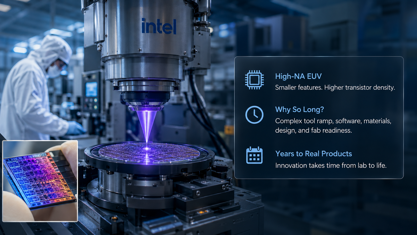
Intel shipped the first High-NA EUV chips
On July 15, ASML confirmed that Intel had become the first company to ship high-volume logic chips manufactured with High-NA EUV lithography. Some of the Core Ultra Series 3 processors going into laptops right now contain layers printed on a machine that, until this year, had never produced a commercial chip.
It is a real milestone. It is also one of those pieces of semiconductor news that gets read backwards — as if a manufacturing breakthrough should show up in hardware prices or upgrade plans this quarter. Probably not. Understanding why is more useful than the headline itself.
What the machine actually does
Chips are made by projecting circuit patterns onto silicon using light. The finer the pattern a machine can resolve, the smaller and denser the transistors, and the more performance fits in the same power budget.
EUV lithography has been in volume production since roughly 2019. High-NA is the next generation of it — “NA” being numerical aperture, essentially how much light the optics can gather and focus. Wider aperture, finer resolution.
The practical payoff is fewer steps. Patterns too fine for standard EUV have to be split across multiple exposures and stitched back together, which adds cost, time, and chances for defects. High-NA can collapse some of that multi-patterning — printing in one exposure, or at least fewer, what used to take several.
These are the most expensive production machines ever built. Samsung’s purchase of two EXE:5200B systems was reported at $773 million, or roughly $386 million each. Only a small number are installed anywhere in the world.
The signals hiding in the wording
The announcement is carefully worded, and the qualifications carry most of the information.
Intel used High-NA on selected layers of 18A, not the whole process, and those layers are described as dual-qualified — they can be produced on either High-NA or standard EUV scanners. Intel kept a path back to the older tools.
That tells us High-NA was not required to build these chips. Intel chose to run real, revenue-generating product through the new machines while retaining a fallback. This is how new lithography generations normally get introduced.
The most substantive claim in the announcement is about yield: ASML says output on the High-NA layers matches its existing EUV platform. That figure comes from the tool vendor — not from Intel, and not from independent measurement — so it is worth holding loosely. If the reported parity holds up in production, it would suggest the learning curve has moved faster than many observers expected, since new lithography usually starts well behind on yield. Until someone outside ASML confirms it, treat it as a vendor claim pointing in a promising direction.
Worth noting who made the announcement. It came from ASML, not Intel. ASML needs a proof point for a tool that other major customers have been slow to commit to, and Intel needs a technology claim it can make against larger foundry competitors. Both parties had reason to publicize this.
This is a 14A story, not an 18A story
The real target is Intel’s next node. 14A is expected to be the first process where High-NA is foundational rather than optional, and shipping product through these machines now is a way of removing risk before that node matters.
Timelines here should be treated with care, because they have moved. Earlier roadmaps pointed to risk production in 2027, while more recent reporting places risk production in 2028 with high-volume manufacturing in 2029. Intel has also indicated that customers will be able to use standard EUV patterning on 14A without redesigning, which is another hedge.
Either way, the node this milestone is really about is years from producing anything.
Why Intel went first — and TSMC didn’t
Being first here was a decision, not an accident. High-NA tools are scarce, only a handful are installed anywhere, and early deployment carries genuine risk. Intel took it because it is trying to reestablish process leadership and sell its foundry business to outside customers, and “first to ship High-NA in volume” is a credential it can point to.
TSMC, the company Intel is chasing, made the opposite call. Its executives have said repeatedly that from 2nm through the A14 node it does not need High-NA, arguing that standard EUV with multi-patterning and computational lithography stays more cost-effective for now. By deferring, TSMC sidesteps billions in tool purchases while Intel absorbs the cost and works down the learning curve.
Both positions can be right at once. Intel is betting that mastering High-NA early pays off at 14A and beyond; TSMC is betting the older approach has more room left in it. The milestone is a real technical achievement and a strategic wager at the same time — which is the honest way to read almost any “industry first.”
Will the next laptop be any cheaper?
Those Core Ultra Series 3 chips are Panther Lake — Intel’s current laptop processors, and the first client parts built on 18A. The line went on sale in laptops in late January, produced mainly at Fab 52 in Arizona. The units carrying High-NA-printed layers are the recent piece ASML flagged, with that work qualified at Intel’s Oregon site. Either way this is real product sold to customers, not a batch of test wafers — Intel is using shipping laptop chips as a low-risk proving ground, running only selected layers through High-NA while keeping the standard path in reserve.
So does printing part of a chip on a more advanced machine make the laptop cheaper? Not here, and not soon.
At this stage the economics run the other way. A High-NA scanner costs roughly twice as much as a standard EUV tool — around $380 million against $180–220 million — and a single High-NA exposure runs about 2.5 times the cost of a standard one. Throughput cuts the same way: because High-NA exposes a smaller field, early tools run fewer wafers per hour than a mature EUV line — roughly 175 against about 195 — so the real cost is not just the machine’s sticker price but how many chips it pushes through in an hour.
The savings only show up when one High-NA pass replaces three or more standard passes on the most complex layers. On simpler layers, the older method is still cheaper. That payoff is targeted at high-volume future nodes, not at a 2026 laptop where only a handful of layers touch the technology at all. And whatever lithography adds or saves is small next to the price of memory, which has climbed for several quarters and pushes finished-system prices in the opposite direction.
Do the math on when this reaches the market
A lithography milestone sits at the very front of a long pipeline, and each stage adds years. Put rough dates on it.
The node this announcement is really about is 14A, with high-volume manufacturing currently projected around 2029. A chip built on it ships in a product, gets qualified and bought by an enterprise sometime after, then serves anywhere from three to seven years — hyperscalers cycle fastest, while much enterprise, government, and telecom gear runs longer — and only then comes off the books and onto the secondary market. That puts the used equipment somewhere in the mid-2030s.
Even 18A — the node already shipping today — follows the same curve. Those machines are entering corporate fleets now and won’t reach disposition in volume until the end of the decade.
So a fab announcement in July 2026 is, for the used-hardware market, a story about the 2030s. That is the gap almost every “what does this mean for hardware” take skips over.
It also explains why refresh cycles ignore process nodes entirely. Nobody replaces a fleet because a new node exists. They replace it when a lease ends, when depreciation runs out, when an operating system loses support, or when a workload finally outgrows the hardware. A new node widens the menu of what’s available to buy. It doesn’t put anything on the buy list — and the used processors and systems trading on the secondary market today were built on nodes two or three generations behind whatever is making headlines.
What to watch next
The follow-up signals on this one are specific. Whether Intel expands High-NA to additional 18A layers or quietly pulls back to standard EUV will say whether the cost math works. Whether TSMC and Samsung accelerate their own High-NA orders will say whether the industry agrees with Intel’s bet. And whether the 14A schedule holds will say whether any of this arrives when Intel says it will.
Those answers land over the next couple of years. The hardware in most server racks today is materially unaffected by all of it.