
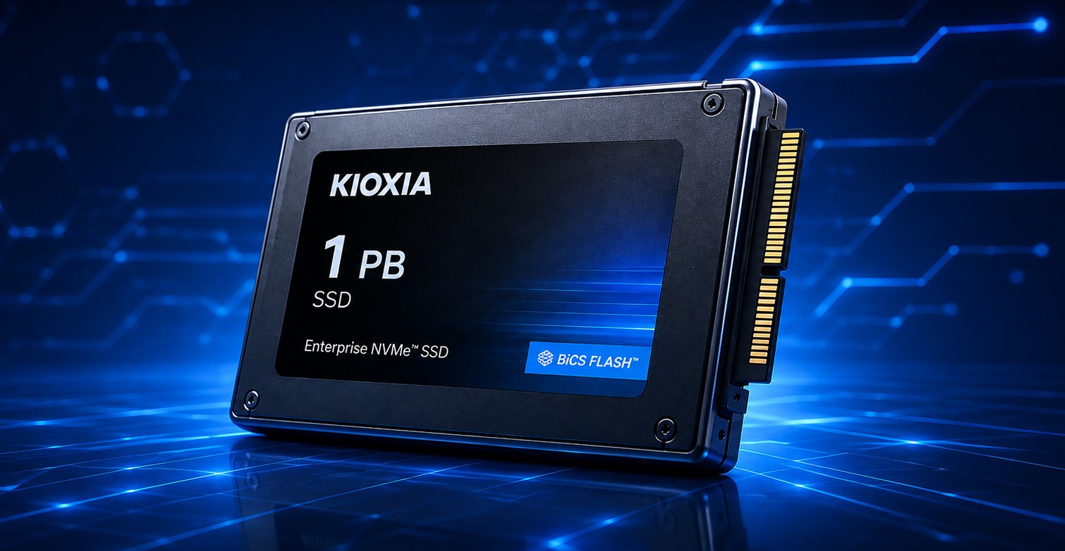
What could the world’s first 1 PB SSD look like?
A petabyte in a single drive has been the storage industry’s next round number for a while. As of this summer, enough of it is on the public record to reconstruct.
At FMS 2026, Kioxia and Sandisk unveiled their 10th-generation QLC 3D flash memory: 332 layers, more than 37 Gb/mm², and up to 60% denser than their 8th-generation part — what the two companies say, on their own survey, is the industry’s highest bit density for QLC NAND. Trade coverage tied it immediately to the world’s first 1 PB SSD, and the connection is fair — this is the flash such a drive would be built from.
No petabyte product was announced, and no ship date exists. But the die capacity is known, the packaging options are published, and a 512 TB drive was on the show floor at the same event. That is enough to model what a petabyte drive would physically be, and to locate where the remaining uncertainty actually sits.
The die: 2 Tb, and it is not a guess
The FMS press release omitted the die capacity, which sent several outlets into estimating it. That was unnecessary. Three weeks earlier, Kioxia had published the development of a 10th-generation 2 Tb 4-bit-per-cell BiCS FLASH device, presented at ISSCC 2026: 332 stacked word lines, 37.6 Gb/mm², write throughput above 85 MB/s.
That is a developed device described in a conference paper, not a part in mass production. But the capacity question is settled: 2 Tb per die, four bits per cell.
Two details in that disclosure are more interesting than the headline density.
The first is a six-plane architecture, a first for the companies’ QLC, arranged in a 1×6 floorplan rather than 2×3. Planes are the independently addressable units inside a die; going from four to six raises how much work a single die can have in flight. The 1×6 arrangement shrinks the bonding-pad region and therefore the die area, which is where a good part of the density gain comes from.
The second is a power technique called Bus Idle Sleep, and Kioxia is explicit about why it exists: in a tall package, the non-selected dies sit idle drawing current while one die is being read or written, and “the recent increase in stack height has led to a greater number of non-selected chips,” making that idle current significant. The fix forces non-selected dies into an internal standby state, cutting idle draw from tens of milliamps to hundreds of microamps.
Idle-current management exists at any stack height. But this is a company explicitly engineering around a problem that grows more important as die stacks grow taller and publishing the fix alongside the die. It is the clearest public signal of where the packaging is heading.
Layer count is the wrong number to watch
Worth a short detour, because it explains why 332 layers beat a taller competitor.
Samsung’s competing V-NAND generation runs more than 400 layers and lands at about 28 Gb/mm². BiCS10 QLC at 37.6 is roughly a third denser with about a fifth fewer layers.
Areal density is the product of three things: stack height, lateral cell pitch, and bits per cell. On-Pitch Select Gate Drain tightens the pitch; QLC encoding adds the fourth bit; CMOS directly Bonded to Array builds logic and memory array on separate wafers and bonds them, removing the thermal constraint tall stacks otherwise impose on the transistors underneath.
Be precise about the split, though. Much of the lead over Samsung is the fourth bit, not the process. Like-for-like, BiCS10 TLC is above 29 Gb/mm² against Samsung’s 28 — a margin of a few percent.
The interface reaches 4.8 Gb/s per I/O pin (4,800 MT/s), using Toggle DDR6.0 and a Separate Command Address protocol that gives control traffic its own path. That is a flash-interface signaling rate, not the throughput of a finished SSD.
A 983.04 TB model: 4,096 dies
Here is the arithmetic that makes a petabyte-class drive concrete. It rests on three assumptions, all of them stated.
Kioxia’s LC9 tops out at 245.76 TB, and the product announcement is specific about the build: a 32-die stack of 2 Tb QLC yielding 8 TB of raw flash in one 154-ball BGA package. Kioxia does not publish the drive’s package count. But enterprise capacities sit on a familiar ladder — 3.84, 7.68, 15.36, 30.72, 61.44, 122.88, 245.76 TB — where advertised decimal capacity runs about 87% of raw binary flash. On that ratio, 245.76 TB usable implies 256 TiB of raw flash: 32 packages, 1,024 dies. A calculation, not a disclosed bill of materials.
If vendors extend the same ladder, the next two doublings from 245.76 TB are 491.52 TB and 983.04 TB — the natural petabyte-class rung. At the same raw-to-usable ratio, 983.04 TB maps to 1,024 TiB of raw flash, which at 2 Tb per die is exactly 4,096 dies.
Hold those three assumptions — 2 Tb dies, LC9-like provisioning, a 983.04 TB target — and the die count is fixed no matter how the drive is assembled. What changes is how the 4,096 get divided:
| Configuration | Packages | Dies per package |
|---|---|---|
| Today’s stack height | 128 | 32 |
| E2-oriented | 64 | 64 |
| Tall-stack | 32 | 128 |
Three axes are available, and a vendor can trade among all of them: die-level scaling raises capacity per die, package-level scaling raises dies per package, board-level scaling raises packages per drive. The petabyte drive will be some combination, and nothing published so far fixes which.
Part of the middle row is already published. Micron describes the emerging E2 form factor as designed around 64 NAND packages — that board-level layout is real. Pairing it with a 64-high 2 Tb stack is this article’s model, not a vendor’s stated plan. The bottom row needs 128-high stacking, four times what ships today, which is the regime Bus Idle Sleep was developed for.
What it will look like from outside
Most likely a ruler rather than 2.5-inch. The LC9 is offered in both, but the drives being shown at half a petabyte are EDSFF only.
E1.L gives a 318.75 mm board. E3.L is much shorter at 142.2 mm but taller and thicker, and E2 — at 200 × 76 mm — was defined specifically to carry more NAND packages than the existing shapes allow.
Interface is genuinely open. Kioxia’s CM10 series is its first PCIe 6.0 enterprise drive and already samples on BiCS10 TLC, so PCIe 6.0 is plausible. It is not established — the largest capacity drive shown this year is still Gen5.
The controller is the least documented piece. Sandisk’s UltraQLC platform is the named vehicle for petabyte drives, using a custom controller with hardware offload engines and a bus multiplexer for very high NAND parallelism. Reporting differs on the specifics: one account reads the Investor Day material as a 64-channel controller, another as a controller scaling to 64 dies per channel. Either way, addressing four thousand dies coherently is its own engineering problem, and no vendor has shown that part working at petabyte scale.
How soon
No committed date exists, but the physical evidence is moving fast.
Sandisk put 1 PB drives on its roadmap at its February 2025 Investor Day, running 128 TB → 256 TB → 512 TB → 1 PB with no year on the final step. Six months later a single-drive 1 PB prototype was on the FMS 2025 floor, described then as still some way out.
The most current datapoint is from this month. DapuStor showed a 512 TB QLC drive at FMS 2026 in E3.L and E2 — PCIe 5.0, double its previous 245 TB design, a petabyte of flash across two drives. No performance specifications, no pricing, no availability date; the claim currently rests on a show-floor demonstration. But it sits in the half-petabyte class immediately below a 1 PB-class device, and it exists as hardware.
So the NAND density is no longer the mystery. What remains unproven in a shipping product is the package stacking, the package count and form factor, the controller implementation, the endurance rating, the thermals and the economics needed to turn roughly 4,096 high-density QLC dies into one manageable drive.
Where a drive like this belongs
Read-heavy tiers, and that is less a limitation than a description of the market.
QLC trades write endurance for density. No endurance specification has been published for BiCS10 QLC at all; for scale, the TLC-based CM10 offers 1 DWPD read-intensive and 3 DWPD mixed-use options up to 61.44 TB.
The workloads pulling on high-capacity QLC are read-dominated by nature: model weights written once and read continuously, training corpora read across epochs, embedding and vector stores, warm and cold data-lake tiers. Those are the deployments where one 245 TB drive replaces a shelf of spinning disks and the write budget never binds. Write-intensive databases, virtualization hosts and heavy log ingest are less obvious candidates until vendors publish endurance and sustained-write figures — QLC suitability depends on write amplification, over-provisioning and controller behavior as much as on the cell type.
The petabyte failure domain
The consequence that gets least attention is the one most likely to shape deployment.
A petabyte drive is a petabyte failure domain. Thirty times the capacity means thirty times the data to reconstruct after a failure, and unless rebuild bandwidth scales in proportion, the window during which the system runs degraded stretches with it. At 30 TB that window is an operational inconvenience. At 983 TB, with production traffic competing for the same fabric, it becomes a design input — the system stays exposed to a second fault for considerably longer.
That ripples through most layers of a storage design. Erasure coding widths and parity counts chosen around 30 TB drives have to be re-evaluated at thirty times the capacity: the math still works, but rebuild duration, failure correlation, repair policy and available bandwidth all feed the model, and the answer moves. Spare capacity gets provisioned as a fraction of a much larger unit. Fabric sized for steady-state traffic has to absorb rebuild bursts measured in hundreds of terabytes. And losing one device takes a meaningful slice of a rack’s capacity offline.
None of this is solved by denser NAND, and it is why a petabyte drive may end up deployed differently from how the capacity headline suggests: fewer per failure domain, more redundancy, and in tiers where a slow rebuild is tolerable. The vendors selling density have relatively little to say about it, which usually means buyers work it out themselves.
What the density buys at rack scale
Density this high changes the shape of a deployment, not just its capacity. Kioxia and Dell showed a 2U configuration scaling to 9.8 PB in May 2026 using forty LC9 E3.L drives; Kioxia’s own comparison for that build claims a comparable system on 30.72 TB drives would need seven more servers and roughly eight times the power — a vendor figure, not an independent measurement. Fill the same forty bays with petabyte-class drives and the chassis holds 40 PB.
Whether that translates into hardware coming out of racks or simply less hardware going into the next expansion depends on how operators use the headroom, and in a tight NAND market the second is at least as likely as the first. Either way it is a demand-side story before it is a supply-side one, and enterprise SSD buying has already reshaped NAND supply in ways that show up well upstream of the rack.
What to watch
Four things, none of them a layer count.
A package announcement above 32 dies high, which is the gating item for the tall-stack path. Production qualification for BiCS10 QLC, as opposed to the ISSCC device. A published DWPD figure, which is what turns 37.6 Gb/mm² into something a storage architect can size. And an actual product at 983.04 TB or the round petabyte above it — from Kioxia, Sandisk, DapuStor or whoever gets the packaging working first.
The flash exists. The form factor exists. The die count is fixed at 4,096. What is still being built is everything between the die and the drive.