NVIDIA Next-Gen NVIDIA Feynman: Defining the Era of Inference Sovereignty and the LPX Revolution
As we approach NVIDIA GTC 2026 (scheduled for March 16–19 in San Jose), the industry is bracing for what CEO Jensen Huang calls processors that will “surprise the world.” For the hardware ecosystem, this isn’t just another product launch; it is the formal pivot from the “Training Era” to the “Inference Sovereignty Era.”
Over the past two years, the narrative has flipped. While training remains a foundational requirement, production-grade agentic inference—real-time chains of reasoning, tool calls, and million-token context windows—has exposed architectural constraints that raw TFLOPS can no longer hide. If the last decade was defined by a war for peak throughput, the coming decade’s battleground will be milliseconds per token (How fast an AI agent can “think” and respond), joules per token(the electrical cost of every word generated), and predictable tail latency (ensuring the AI doesn’t “stutter” during complex reasoning) at batch size = 1.
Below, we evaluate the hardware, packaging, storage, and supply-chain signals—including the newly rumored Intel Foundry partnership—that make the Feynman roadmap the most ambitious in semiconductor history.
1. The Economics of Token-Level Latency
Large language models (LLMs) are no longer just static backends; they are instrumented inside products as online agents. These agents rarely use massive batch sizes when interacting with single users. Instead, they stream tokens, perform stepwise “Chain of Thought” reasoning, and execute external tool calls.
When an agent executes 30–80 sequential reasoning steps, every millisecond of tail latency (p95 or p99) compounds into a visible UX stall. Optimizing for latency at batch = 1 is a fundamentally different engineering challenge than optimizing for bulk training throughput.
The industry has hit the “Stochastic Wall.” In traditional GPU architectures, shared on-chip resources create contention—an unpredictable pattern of data movement across the fabric. That contention produces jitter: variance in latency caused by data packets competing for the same physical interconnects. While this variability is tolerable for chatbots, it becomes fatal for agentic AI swarms that depend on tightly synchronized, millisecond-precise feedback loops.
Reporting throughout early 2026 suggests NVIDIA’s GTC keynote will prioritize low-latency inference designs over the pure “FLOPS races” that characterized the Blackwell Ultra era.
Market Intelligence: Industry reporting in Q1 2026 (via Chosun Biz and TrendForce) suggests a strategic pivot at GTC 2026. While the Blackwell Ultra era was defined by achieving the highest possible FLOPS for model training, the new Rubin and Feynman roadmaps prioritize ‘Inference Sovereignty’—minimizing tail latency to enable real-time Agentic AI swarms.
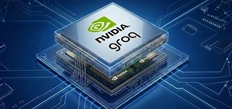
2. Deterministic Decode: The $20 Billion Groq Integration
The move from rumor to public disclosure in late 2025 confirmed a landmark $20 billion asset deal between NVIDIA and Groq. NVIDIA’s decision to license Groq’s LPU technology and integrate its leadership into a specialized inference engineering team confirms that deterministic logic is now a core pillar of the roadmap. This transition, widely expected to debut as part of the Feynman architecture at GTC 2026, marks the end of ‘stochastic’ (unpredictable) AI hardware.
The Hardware/Software Contract
Deterministic dataflow cores replace hardware’s dynamic run-time scheduling with compiler-driven, cycle-accurate execution.
-
Dynamic (Traditional): The hardware decides on-the-fly where to send data, like an airport tower managing unpredictable traffic. This leads to “resource contention,” where data must wait for a core to become free, creating variable timing (jitter).
-
Deterministic (Feynman): The compiler acts as a master architect, laying out a “robotic assembly line” where every datum arrives at a specific transistor at a pre-calculated nanosecond. There are no traffic jams because there are no “decisions” made at runtime.
This creates a near-constant p95 latency envelope. For enterprises, this means “Sovereignty” over their Service Level Agreements (SLAs): you no longer just hope for a fast response; the hardware guarantees it.
3. Feynman Architecture: The 1.6nm Vertical Fusion
Named after physicist Richard Feynman—who famously declared “There’s plenty of room at the bottom“—this 2028 architecture is built on TSMC’s A16 (1.6nm) node. This represents the current technical limit of modern silicon fabrication.
The Super Power Rail (BSPD)
The breakthrough of the Feynman generation lies in Backside Power Delivery (BSPD), which TSMC brands as the Super Power Rail.
-
The Problem: In current 4nm and 3nm chips, power lines and signal lines compete for space on the “front” of the wafer. This causes routing congestion and voltage drops.
-
The Solution: BSPD moves the entire power delivery network to the backside of the wafer.
By separating “power” from “data,” NVIDIA can utilize Hybrid Bonding to enable ultra-dense, logic-on-logic stacking. This allows Feynman to stack SRAM-rich LPX chiplets directly over the compute die, effectively eliminating the physical distance that causes latency in inter-chip communication.
4. SRAM Locality: The pJ/bit Energy Battle
5. The Memory Fabric: 100M IOPS SSDs
As context windows grow to millions of tokens, the “Memory Wall” becomes a physical barrier. To solve this, NVIDIA is collaborating with SK Hynix and Kioxia on “AI SSDs” designed specifically for AI inference.
These devices, code-named “Storage Next,” target a staggering 100 million random read IOPS, which is roughly 33 times faster than today’s high-end enterprise SSDs.
-
Technology: These drives utilize XL-Flash or High Bandwidth Flash (HBF).
-
Peer-to-Peer Mode: They connect via PCIe 7.0, allowing the GPU to access the SSD directly without CPU intervention.
This allows an AI agent to “swap” between a massive “long-term memory” (stored on the SSD) and the “active SRAM” with minimal delay. By the time Feynman launches, the SSD will no longer be “slow storage”—it will be a peer to the GPU’s memory pool.
6. Silicon Photonics and Co-Packaged Optics (CPO)
When clusters scale to thousands of nodes, the “network” itself becomes a source of jitter. Traditional copper cables are power-hungry and introduce serialization latency.
NVIDIA’s Spectrum-X Ethernet Photonics and Quantum-X InfiniBand solutions, expected to ship in late 2026, introduce Co-Packaged Optics (CPO).
-
Integration: CPO embeds the optical engine directly alongside the switch ASIC or GPU.
-
Efficiency: This reduces per-port power consumption and removes the need for digital signal processing (DSP) retimers.
In the Feynman era, a cluster may dedicate specific racks to “Prefill” (compute-heavy) and others to “Decode” (latency-heavy), using an optical fabric to move data between them at the speed of light.
7. Software: The NVIDIA Dynamo & NIXL Frameworks
Hardware determinism is useless without software that can orchestrate it. Traditional CUDA programming hides the hardware to make it easier for developers, but deterministic hardware requires explicit control.
NVIDIA is solving this with the NVIDIA Dynamo framework, an open-source, modular inference framework. A key component of this is NIXL (NVIDIA Inference Transfer Library), which handles point-to-point communication in distributed environments.
How Dynamo Drives the Feynman Roadmap:
-
Disaggregated Serving: It splits the inference process. The “Prefill” (the heavy lifting of understanding the prompt) happens on standard GPU cores.
-
Asynchronous Transfer: NIXL moves the resulting “KV cache” (the model’s memory of the prompt) to the deterministic LPX cores.
-
Deterministic Generation: The actual token generation happens on the LPX cores, ensuring a perfectly smooth stream of text for the user.
Without this software convergence, the deterministic speed of the Feynman cores cannot be realized in a production environment.
8. Architectural Roadmap: Blackwell to Feynman
To understand the leap Feynman represents, we must look at how specifications have evolved. This transition marks the shift from “evolutionary” node shrinks to “revolutionary” architectural fusions.
| Feature | Blackwell Ultra (2025) | Vera Rubin (2026) | Feynman (2028) |
| Primary Node | 4nm (TSMC) | 3nm (TSMC N3P) | 1.6nm (TSMC A16) |
| Logic Type | Stochastic GPU | Hybrid (Rubin CPX) | Deterministic LPX |
| Power Routing | Front-side | Front-side | Backside (Super Rail) |
| Packaging | CoWoS-L | CoWoS-R / SoIC | 3D Stacked Logic |
| HBM Generation | HBM3e | HBM4 (288GB) | HBM4e + SRAM |
| I/O Sourcing | TSMC | TSMC | Intel 18A (Rumored) |
| Interconnect | NVLink 5 | NVLink 6 (3.6 TB/s) | Photonics / CPO |
| Efficiency | $1.0\times$ (Baseline) | $5.0\times$ | $100.0\times$ (Projected) |
The move to the A16 node and Backside Power is the primary driver for that $100\times$ efficiency target. By moving power to the back, the chip generates less heat and experiences less electrical resistance, allowing for much higher clock speeds and denser stacking.
9. Market and Secondary-Market Implications
For companies specializing in hardware resale, like buysellram.com, the Feynman generation introduces a significant bifurcation of asset classes.
Faster Depreciation of “Specialized” Nodes
Deterministic, SRAM-heavy accelerators like those in the Feynman roadmap are “fixed-function” appliances. They excel at inference but are less flexible than a general-purpose GPU like the H200 or B200.
-
The Consequence: These specialized inference machines may have a smaller buyer pool in the secondary market once they are superseded, potentially leading to faster depreciation compared to “flexible” compute assets.
The Rise of Integrated Providers
The shift toward CPO and logic stacking makes hardware harder to service or upgrade at the component level. As the GPU, memory, and optics become a single “fused” unit, the secondary market will likely move away from individual “RAM” or “GPU” sales and toward full-rack or full-blade lifecycle management.
10. What to Watch for at GTC 2026
If you are attending the keynote on March 16, watch for these specific validation points:
-
Process Maturity: Does NVIDIA show silicon references for the A16 node or demonstrate the stability of the Super Power Rail (BSPD)?
-
Groq/LPU Integration (LPX): Look for concrete benchmarks showing “Deterministic Latency” or “LPX Core” counts in the new Rubin-Next or Feynman previews.
-
Storage Fabric: Are there live demos of the 100M IOPS “Storage Next” SSDs running in a peer-to-peer mode with GPUs?
-
Software Ecosystem: Look for the public release of NVIDIA Dynamo 2.0 and its support for heterogeneous (GPU + LPX) clusters.
Conclusion: The New Standard of Precision
NVIDIA’s pivot at GTC 2026 marks the end of the “brute force” era. As the roadmap moves from the stochastic Blackwell Ultra to the deterministic Feynman and Rubin architectures, the primary metric is no longer raw FLOPS, but guaranteed latency. For the modern enterprise, “Inference Sovereignty” is now the prerequisite for deploying reliable, autonomous Agentic AI.
Staying competitive in the 1.6nm “Angstrom” era requires a deterministic hardware stack. If your current infrastructure is creating the “latency jitter” that stalls complex reasoning chains, now is the time to cycle that capital. To fund your transition to Feynman-class systems, you can leverage a data center GPU buyback program to capture maximum value before the industry fully standardizes on deterministic logic. In the next phase of the AI race, speed is expected—but precision is the prize.